Understanding printed circuit boards (PCB) is an important factor in computing nowadays. You will require to get habituated with these green sheets and know how they function if you ever expect to make a working computer or another electronic device.
PCB design is one of the most crucial design elements inside the design of electronics products. For maximum cases, an electronics hardware design engineer will design the circuit. After that, a printed circuit board layout expert will take on the printed circuit board layout and design from a schematic delivered using a printed circuit board CAD system.
Your time is precious. That is why you need to design your PCB properly from the beginning. In our guide, we have covered all the things you require to know about printed circuit board (PCB) design layout.
What is a Printed Circuit Board?
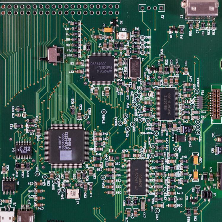
A Printed Circuit Board (PCB), sometimes referred to as a Printed Wiring Board or a Printed Wiring Card. It is a stiff structure that includes electrical circuitry built of embedded metal wires called traces, and bigger parts of metal called planes. A PCB is a board that describes the work of an electrical or mechanical wire structure of the circuit.
This board comprises substrates with copper tracks that work as wires to which components are attached. Electronic elements are soldered onto the PCB so that they are firmly held. Insulating and copper layers on the board have indicator symbols for energy supply and ground.
Maximum electronic or mechanical devices and appliances work because of the guidelines produced on the printed circuit board. It indicates that the printed circuit board is the core of these systems. Also, if the electronic circuits in these systems are not made on a good printed circuit board design or layout, the system won’t function.
A basic guide on designing a printed circuit board layout
Although the basics of printed circuit boards look easy in the beginning, when you start to design your circuit boards the difficulties are observed rapidly. Designing a printed circuit board layout can be complex, and it is simple to avoid crucial steps. Some crucial factors to consider when designing your printed circuit board layout are given below.
The Schematics
The schematic of your printed circuit board design is the diagram that displays how all the things are laid out and linked together. Whereas the layout displays where every component is located, the schematic also displays how every component is linked together. In addition, the schematic shows how electricity flows all over the printed circuit board.
High-frequency circuit boards
High-frequency circuit boards are complex, compactly wired, classic printed circuit boards usually used in communications, manufacturing, and medical industries. Those printed circuit board designers who concentrate on high-frequency circuits should be industrious regarding the layout of their boards. They also should concentrate on the various special considerations a high-frequency printed circuit board requires.
The routing of PCB and location of components
How every part of your PCB is routed jointly and where they have located impacts the heat delivery, weight, performance, and durability of the PCB. It is significant to take care to make a design that uses the finest practices. As a result, your printed circuit board will function properly, and will not fail early.
A work of art and science
When you are making your PCB, you can combine your preferred style, creativity, and concepts to complement the science behind your design. While there are a few general rules, the most groundbreaking new products and schematics are created by people who include their exceptional view when bringing a concept to life.
Conclusion
When it comes to PCB, this is only the start of your journey. There is a huge amount of knowledge available on the internet for free. Therefore, you are no longer restricted by the barricades of expensive higher education. As you can realize from this article, printed circuit board layout design is a complex thing to do perfectly.
You need to consider spacing, traces, component location, and several other aspects. Learning the basic terms, knowing the available software and the strengths of all, and obeying the easy steps described above can make printed circuit board layout design much less complex.